Material science explores the properties and applications of materials by manipulating their structure at the atomic or molecular level, enabling innovations in durability, conductivity, and flexibility. Nanophotonics focuses on the behavior of light on the nanometer scale and its interaction with nanostructures, driving advancements in imaging, sensing, and optical communication. Both fields converge in developing new materials with tailored optical properties, enhancing technologies such as photonic devices and nanolasers.
Table of Comparison
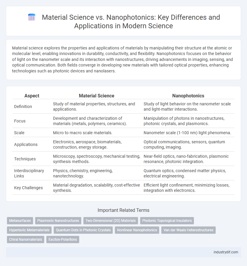
| Aspect | Material Science | Nanophotonics |
|---|---|---|
| Definition | Study of material properties, structures, and applications. | Study of light behavior on the nanometer scale and light-matter interactions. |
| Focus | Development and characterization of materials (metals, polymers, ceramics). | Manipulation of photons in nanostructures, photonic crystals, and plasmonics. |
| Scale | Micro to macro scale materials. | Nanometer scale (1-100 nm) light phenomena. |
| Applications | Electronics, aerospace, biomaterials, construction, energy storage. | Optical communications, sensors, quantum computing, imaging. |
| Techniques | Microscopy, spectroscopy, mechanical testing, synthesis methods. | Near-field optics, nano-fabrication, plasmonic resonance, photonic integration. |
| Interdisciplinary Links | Physics, chemistry, engineering, nanotechnology. | Quantum optics, condensed matter physics, electrical engineering. |
| Key Challenges | Material degradation, scalability, cost-effective synthesis. | Efficient light confinement, minimizing losses, integration with electronics. |
Introduction to Material Science and Nanophotonics
Material Science explores the properties, structure, and performance of materials, enabling the development of novel substances with tailored characteristics for diverse applications. Nanophotonics investigates light-matter interactions at the nanoscale, exploiting quantum and electromagnetic phenomena to manipulate photons in devices such as plasmonic sensors and photonic crystals. Integrating Material Science with Nanophotonics drives innovations in optoelectronics, enhancing the efficiency and functionality of nanoscale optical components.
Fundamental Principles of Material Science
Material science explores the fundamental principles governing the structure, properties, and behavior of materials at the atomic and molecular levels, emphasizing crystallography, phase transitions, and defect chemistry. Nanophotonics leverages these material properties to manipulate light-matter interactions at the nanoscale, relying on quantum confinement effects and plasmonic resonances. Understanding band theory and electron mobility in semiconductors is crucial for developing advanced nanophotonic devices with tailored optical functionalities.
Core Concepts in Nanophotonics
Nanophotonics explores the behavior of light on the nanometer scale, focusing on manipulating photons using nanostructures and materials with unique optical properties. Core concepts include plasmonics, photonic crystals, and metamaterials, which enable control over light-matter interactions beyond the diffraction limit. These advanced phenomena diverge from traditional material science by emphasizing quantum effects and nanoscale optical confinement, critical for innovations in imaging, sensing, and communication technologies.
Key Materials Used in Nanophotonics
Key materials used in nanophotonics include plasmonic metals such as gold and silver, which enable strong light-matter interactions at the nanoscale. Semiconductor nanostructures like quantum dots and nanowires provide tunable optical properties essential for nanoscale photonic devices. Dielectric materials with high refractive indices, including silicon and gallium nitride, are crucial for developing low-loss nanophotonic components and metasurfaces.
Intersection of Material Science and Nanophotonics
The intersection of material science and nanophotonics enables the manipulation of light-matter interactions at the nanoscale, leading to the development of advanced photonic materials with tailored optical properties. Employing nanostructured materials such as metamaterials, plasmonic nanoparticles, and photonic crystals, researchers achieve unprecedented control over light propagation, absorption, and emission. This synergy drives innovations in applications like high-efficiency solar cells, optical sensors, and quantum information technologies.
Analytical Techniques in Material Science and Nanophotonics
Analytical techniques in material science, such as X-ray diffraction (XRD) and scanning electron microscopy (SEM), enable detailed characterization of crystal structures and surface morphologies, providing critical insights into material properties. In nanophotonics, techniques like near-field scanning optical microscopy (NSOM) and photoluminescence spectroscopy are essential for investigating light-matter interactions at the nanoscale, revealing optical behaviors unique to nanostructures. Both fields leverage advanced spectroscopic methods, yet material science prioritizes structural analysis while nanophotonics focuses on optical and electronic phenomena at nanometer resolutions.
Applications in Optoelectronics and Photonic Devices
Material science advances in synthesizing novel compounds with tailored electronic and optical properties directly enhance nanophotonics by enabling precise control of light-matter interactions at the nanoscale. Applications in optoelectronics benefit from engineered materials such as perovskites and 2D transition metal dichalcogenides, which improve the efficiency and tunability of photonic devices like LEDs, lasers, and photodetectors. The synergy between material innovations and nanophotonic structures drives breakthroughs in ultrafast modulation, energy harvesting, and on-chip optical communication technologies.
Challenges in Integrating Material Science with Nanophotonics
Integrating material science with nanophotonics faces significant challenges related to the precise synthesis and manipulation of nanomaterials with tailored optical properties at atomic scales. Achieving uniformity and stability in nanoscale photonic devices often requires overcoming issues such as surface defects, quantum confinement effects, and material compatibility. Advanced characterization techniques and novel fabrication methods are essential to address these obstacles and enable practical applications in photonic circuits and sensors.
Recent Advances and Emerging Trends
Recent advances in Material Science have enabled the development of novel metamaterials with unprecedented optical properties, directly impacting the field of Nanophotonics through enhanced light manipulation at the nanoscale. Emerging trends highlight the integration of two-dimensional materials like graphene and transition metal dichalcogenides, which offer tunable electronic and photonic characteristics crucial for next-generation nanophotonic devices. Cutting-edge research emphasizes scalable fabrication techniques and the exploration of quantum effects to drive innovations in energy harvesting, sensing, and information processing applications.
Future Directions and Industry Outlook
Material Science advances in developing novel nanomaterials with tailored electronic and optical properties essential for next-generation nanophotonic devices. Future directions include integrating two-dimensional materials and metamaterials to enhance light-matter interactions at the nanoscale, enabling breakthroughs in quantum computing and ultrafast communication. Industry outlook focuses on scalable fabrication techniques and hybrid material platforms to drive commercial adoption in photonic circuits, sensors, and energy-efficient optoelectronics.
Related Important Terms
Metasurfaces
Metasurfaces, engineered two-dimensional materials with subwavelength features, bridge Material Science and Nanophotonics by enabling unprecedented control over light-matter interactions at the nanoscale. Their unique electromagnetic properties arise from precisely designed nanoantennas, facilitating applications in optical computing, sensing, and holography.
Plasmonic Nanostructures
Plasmonic nanostructures are engineered at the nanoscale to manipulate light-matter interactions beyond the diffraction limit, playing a critical role in both material science and nanophotonics by enabling enhanced optical phenomena such as surface plasmon resonance and localized field confinement. Their integration into advanced materials enhances applications in sensing, photothermal therapy, and nonlinear optical devices by exploiting the unique electromagnetic properties arising from collective electron oscillations in metals like gold and silver.
Two-Dimensional (2D) Materials
Two-dimensional (2D) materials such as graphene and transition metal dichalcogenides have revolutionized both material science and nanophotonics due to their exceptional electronic, mechanical, and optical properties. In material science, 2D materials enable the development of ultrathin, flexible devices, while in nanophotonics, their strong light-matter interactions facilitate advancements in plasmonics, photodetection, and quantum optics.
Photonic Topological Insulators
Photonic topological insulators, emerging at the intersection of material science and nanophotonics, exhibit robust light propagation immune to defects due to their unique topological properties. Advances in engineered metamaterials enable the manipulation of light at the nanoscale, fostering innovations in non-reciprocal photonic devices and enhanced optical communication systems.
Hyperbolic Metamaterials
Hyperbolic metamaterials, architected with anisotropic subwavelength structures, exhibit extraordinary optical properties such as negative refraction and enhanced photonic density of states, driving advancements in nanophotonics for applications like super-resolution imaging and spontaneous emission control. Material science plays a crucial role in synthesizing these metamaterials with precise nanoscale architectures, leveraging techniques like atomic layer deposition and electron beam lithography to tailor their hyperbolic dispersion and optimize performance in photonic devices.
Quantum Dots in Photonic Crystals
Quantum dots embedded in photonic crystals exhibit unique optical properties by manipulating light at the nanoscale, enhancing emission efficiency and enabling precise wavelength control. Material science advances in synthesizing uniform quantum dots and fabricating defect-free photonic crystals are critical for optimizing light-matter interaction in nanophotonic devices.
Nonlinear Nanophotonics
Nonlinear nanophotonics exploits the unique properties of nanostructured materials to manipulate light-matter interactions at the nanoscale, enabling ultrafast signal processing and enhanced harmonic generation beyond the limitations of bulk material science. Advances in engineered metamaterials and plasmonic nanostructures drive breakthroughs in nonlinear optical responses, crucial for next-generation photonic devices and quantum information technologies.
Van der Waals Heterostructures
Van der Waals heterostructures in material science exploit atomically thin layers with strong interlayer interactions to engineer novel electronic and optical properties. In nanophotonics, these heterostructures enable precise control of light-matter interactions at the nanoscale, enhancing device performance in photodetectors, modulators, and quantum emitters.
Chiral Nanomaterials
Chiral nanomaterials represent a pivotal intersection between material science and nanophotonics, leveraging their unique optical activity to manipulate circularly polarized light at the nanoscale. These materials enable breakthroughs in enantioselective sensing, photonic devices, and metamaterials by exploiting their distinct chiroptical properties, which are intrinsically linked to their nanoscale structural asymmetry.
Exciton-Polaritons
Exciton-polaritons represent hybrid quasiparticles arising from strong coupling between excitons in semiconductors and photons in optical microcavities, bridging material science and nanophotonics through their unique light-matter interactions. Their manipulation enables advancements in low-threshold lasers, quantum information processing, and nonlinear optical devices, positioning them as pivotal elements in both fundamental research and applied photonic technologies.
Material Science vs Nanophotonics Infographic